-
Phone
+86 18268068123
-
Address
Industrial Village, Langxia Town, Yuyao City, Zhejiang Province
-
E-mail
The Invisible Edge: Where Precision Meets Perfection
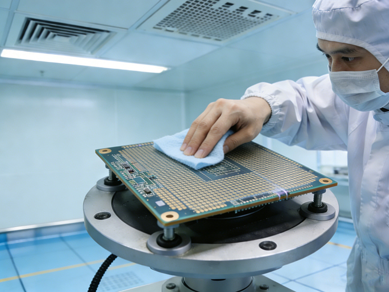
Even in environments where the air is counted particle by particle, your greatest contamination risk may be the tool you trust to clean. Are you confident that every wipe, every contact, leaves your process closer to perfection—not farther away?
The Hidden Costs of "Clean"
Micro-Abrasions & Latent Defects: Standard materials leave microscopic scratches on optical surfaces, polished silicon, or delicate coatings, creating failure points invisible until final inspection.
Sub-Micron Residue: Fibers and particles shed during cleaning become the stubborn contaminants on lenses, photomasks, and wafer surfaces, directly impacting yield and performance.
Electrostatic Discharge (ESD) Threats: Non-dissipative materials generate uncontrolled static, attracting airborne particles or causing sudden discharges that damage sensitive micro-electronics.
Unpredictable Performance: Inconsistent material quality forces constant process adjustment, undermining the repeatability and data integrity that precision manufacturing demands.
Redefining Contact at the Microscopic Level
We engineer our ultra-fine fiber nonwovens not as mere wipes, but as deterministic, predictable components of your precision process.
1. Engineered for Zero-Impact Contact:
Our proprietary blend of sub-micron fibers (0.1-0.5 denier) creates a surface softer than a fingerprint. It cleans with molecular-level gentleness, eliminating the risk of abrasion on the most sensitive substrates, from diamond-turned optics to bare silicon wafers.
2. The Science of True Capture, Not Redistribution:
Unlike materials that push contaminants, our high-surface-area microfiber structure acts as a high-efficiency particulate trap. Combined with laser-sealed edges that prevent fiber shedding, it removes contamination at the source, validated by IEST-RP-CC004.3 testing protocols.
3. Inherent, Permanent Static Control:
We integrate permanent conductive elements directly into the fiber matrix, providing stable, humidity-independent surface resistivity (10⁶–10⁹ Ω/sq). This built-in safety ensures the secure handling of semiconductor components, MEMS devices, and read/write heads.
4. Predictability Engineered In:
From basis weight and thickness to solvent resistance and low extractables, every parameter is controlled and documented. We provide the consistent, batch-to-batch reliability required to make your cleaning process a controlled variable, not an unknown risk.
Application-Specific Solutions for Critical Processes
Optics & Photonics: Our silicon-, latex-, and amonia-free formulations guarantee pristine surfaces for laser optics, EUV lithography components, and AR/VR lens assembly.
Semiconductor & Advanced Packaging: Grades engineered for ultra-low ionic contamination (Na⁺, Cl⁻, SO₄²⁻) and high purity for FPC/PCB cleaning, die-attach surface prep, and vacuum chamber maintenance.
Medical Device & Diagnostics: Biocompatible, USP Class VI-certified materials for cleaning surgical robotics, imaging sensors, and in-vitro diagnostic cartridges.
Critical Surface Preparation: Formulations with superior solvent holdout and chemical compatibility for CMP pad conditioning, thin-film coating prep, and bonding surface activation.
The Tangible ROI of Precision Cleaning
Choosing Lonson ultra-fine fiber nonwovens is an investment in:
Yield Protection: Minimize random defects and scrap caused by cleaning-induced contamination and damage.
Process Control: Achieve predictable, repeatable results that strengthen your quality management system.
Risk Mitigation: Eliminate ESD events and chemical cross-contamination that lead to costly rework or field failures.
Total Cost of Ownership: Optimize consumption with higher efficiency materials and reduce costs associated with yield loss and process variability.
In the world of nanometers and photons, there is no room for compromise. Your cleaning material shouldn't be the largest particle in the room.
Engineered for the Margin of Error That Doesn't Exist.
[Download Our Technical White Paper: "The Correlation Between Wipe Material Science and Precision Manufacturing Yield" or Request a Validation Sample Kit Tailored to Your Application.]